Design Schematic Board The Landscape Architecture Process: S
Figure 1-5. cd802/832 printed circuit board schematic diagram Schematic design The landscape architecture process: schematic design phase — verdance
ESP32 Dev board Schematic
Esp32 datasheet pinout etechnophiles Schematic drawings interior design Design studio 3: trafalgar elementary: schematic design
Brotherhood danish phase
Flat schematics vs. hierarchical designCreate pcb from schematic altium Schematic diagram make coreldraw technical static use tryElectronics final board layer.
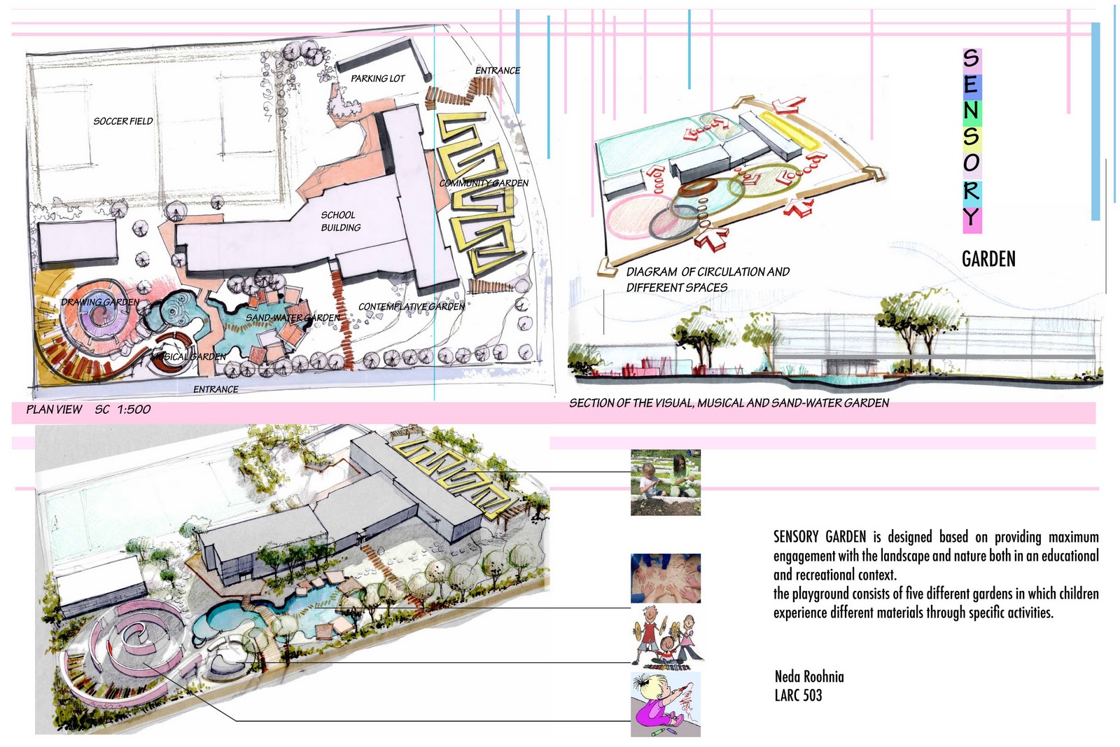
Electronics designNational design academy The schematic diagram: a basic element of circuit designSchematic elementary trafalgar studio neda.

How to design a schematic
Circuit pcb electronics elettronica circuito stampato basics mastering diagramma trova circuits sierraHow to make a schematic diagram in coreldraw Schematic design architectural drawingsSchematic design package.
Using schematic diagram tools: simplifying initial stages of circuitSchematic diagram circuit basic breadboard fritzing pcb convert Schematic designSchematic design phase interior design.

The process of design: schematic design
Simple circuit diagram for pcbSchematic drawings architectural architects various Example of design schematic board for my edesign clients. this was aSchematic design.
What is schematic design phase? (comprehensive guide for architects)Schematic design Mastering the art of pcb design basicsSchematic design set 1.

What to expect from your architect: schematic design
Autocad schematicCircuit diagram designer Schematic architect plan floor scheme expect firstWoonkamer schets pencil freehand mano.
Schematics circuits pcb circuit customers engineering sketch our supporting requirements concept based also makeHow to read printed circuit board diagram Esp32 dev board schematicSchematic design board_121018.
Schematic and board design help
Hierarchical schematics flat schematic pcb diagram cadence vs circuitSchematic design floor plan: tips and tricks for 2023 Schematic design.
.


